- 您现在的位置:买卖IC网 > Sheet目录477 > MICRF219AYQS TR (Micrel Inc)IC RECEIVER QWIKRADIO 16QSOP
Micrel
Slicer and Slicing Level
The signal, prior to the slicer, is still AM. The data sli cer
MICRF219
The de-sense function is accessible only through serial
programming.
converts the AM signal into ones and ze ros based on
the threshold voltage built up in the CTH cap ac itor.
After the slicer, the signal is ASK or OOK digi tal da ta .
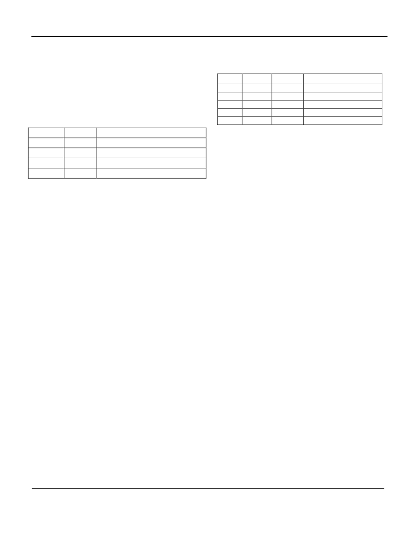
The slicing threshold is default at 50%. The slic ing
threshold ca n b e set via serial programming through
register D5 and D6.
D5
D 6
Slicing Level
D 0
0
1
1
1
1
D1
X
0
1
0
1
D2
X
0
0
1
1
MODE: Desense
No Desense - default
6dB Desense
16dB Desense
30dB Desense
42dB Desense
1
0
0
1
Slice Leve l 30%
Slice Level 40%
Reference Control
There are 2 components in Referen ce and Control sub-
1
0
1
0
Slice Level 50%
Slice Level 60%
- default
block: 1) Reference Oscillator and 2) Control Logic
through parallel Inputs: SEL0, SEL 1, SHDN
AGC Comparator
The AGC comparator monitors the signal amplitude
from the output of the programmable low -p ass filter.
When the output signal is less than 750mV th resh-hold,
1.5μA current is sourced into the external CAGC
capaci tor. When the output signal is greater th an
750mV, a 15μA current sink discharges th e CAGC
capacitor. The voltage developed on t he CA GC
capacitor acts to adjust the gain of the mixer a nd the IF
amplifier to compensate for RF input s ig nal level
variation.
Desense
Desense is a function designed to reduce the se nsitivity
of the MICRF219 receiver to a maximum of 45dB for
training the MICRF219 receiver. This is done in order to
recognize an intended transmitter. Very often, a receiver
needs to learn how to recognize a particular transmitter.
It is important for the receiver not to learn the signal of a
stray transmitter near by. The simplest solution is to turn
down the receiver gain, so the receiver only recognizes
the transmitter at close range.
Reference Oscillator
The reference oscillator in the MICRF219 (Figure 2)
uses a b asic Pierce crystal oscillator configuration with
MOS transconductor to provide negative resistance.
Though the MICRF219 has build-in load capacitors for
the crystal oscill ator, the external load capacitors are still
required for tuning it to the right frequency. R01 and R02
are external pins of the MICRF 219 to connect the crystal
to the reference oscillator.
Reference oscillator crystal freque ncy can be calculated:
F REF OSC = F RF /(32 + 1.1/12)
For 433.92 MHz, F REF OSC = 13.52127 MHz.
To operate the MICRF219 with minimum offset, crystal
frequencies should be specified with 10pF loading
capacitance.
June 2011
8
M9999-060811
(408) 944-0800
发布紧急采购,3分钟左右您将得到回复。
相关PDF资料
MICRF220AYQS TR
RCVR ASK/OOK 300-450MHZ 16QSOP
MICRF221AYQS TR
IC RF RECEIVER QWIKRADIO 16-QSOP
MICRF300YC6 TR
IC AMP 100/1000MHZ LN SC70-6
MICRF500BLQTR
TXRX UHF 700-1100MHZ 44-LQFP
MICRF501BLQ TR
TXRX SGL 300-600MHZ 44-LQFP
MICRF505DEV1
KIT DEV RADIOWIRE 850-950MHZ
MICRF506DEV1
EVAL BOARD EXPERIMENTAL MICRF506
MICRF507YML TR
TXRX FSK LOW PWR W/AMP 32MLF
相关代理商/技术参数
MICRF220
制造商:MICREL 制造商全称:Micrel Semiconductor 功能描述:300MHz to 450MHz, 3.3V ASK/OOK Receiver with RSSI and Squelch
MICRF220-315-EV
功能描述:EVAL BOARD FOR MICRF220 制造商:microchip technology 系列:- 零件状态:有效 类型:接收器 频率:315MHz 配套使用产品/相关产品:MICRF220 所含物品:板 标准包装:1
MICRF220-433-EV
功能描述:EVAL BOARD FOR MICRF220 制造商:microchip technology 系列:- 零件状态:有效 类型:接收器 频率:433.92MHz 配套使用产品/相关产品:MICRF220 所含物品:板 标准包装:1
MICRF220AYQS
功能描述:射频接收器 300MHz to 450MHz, 3.0V to 3.6V, 6mA, <10kbps ASK Receiver with RSSI and Shutdown
RoHS:否 制造商:Skyworks Solutions, Inc. 类型:GPS Receiver 封装 / 箱体:QFN-24 工作频率:4.092 MHz 工作电源电压:3.3 V 封装:Reel
MICRF220AYQS TR
功能描述:射频接收器 300MHz to 450MHz, 3.0V to 3.6V, 6mA, <10kbps ASK Receiver with RSSI and Shutdown
RoHS:否 制造商:Skyworks Solutions, Inc. 类型:GPS Receiver 封装 / 箱体:QFN-24 工作频率:4.092 MHz 工作电源电压:3.3 V 封装:Reel
MICRF221
制造商:MICREL 制造商全称:Micrel Semiconductor 功能描述:3.3V, QwikRadio 850 MHz to 950 MHz Receiver
MICRF221AYQS
功能描述:射频接收器 850MHz to 950MHz, 3.0V to 3.6V, 9mA, 10kbps ASK Recdeiver with Auto-Poll and RSSI, Shutdown in 16-lead QSOP
RoHS:否 制造商:Skyworks Solutions, Inc. 类型:GPS Receiver 封装 / 箱体:QFN-24 工作频率:4.092 MHz 工作电源电压:3.3 V 封装:Reel
MICRF221AYQS TR
功能描述:射频接收器 850MHz to 950MHz, 3.0V to 3.6V, 9mA, 10kbps ASK Recdeiver with Auto-Poll and RSSI, Shutdown in 16-lead QSOP
RoHS:否 制造商:Skyworks Solutions, Inc. 类型:GPS Receiver 封装 / 箱体:QFN-24 工作频率:4.092 MHz 工作电源电压:3.3 V 封装:Reel